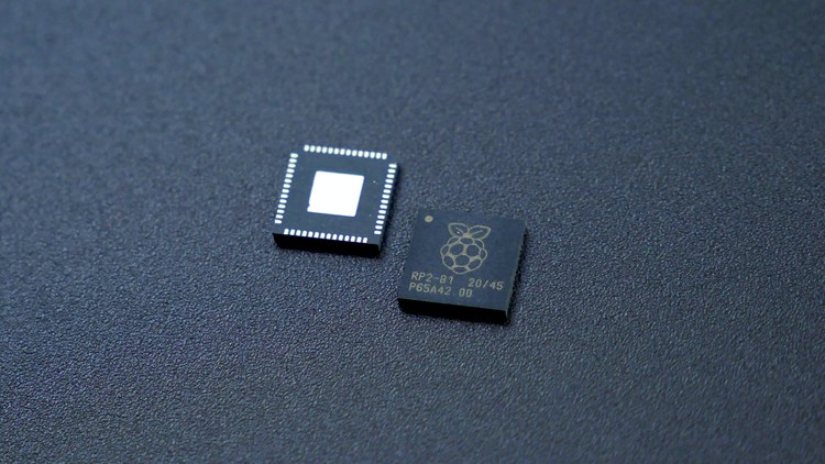
Learn the principles, concepts and design methodologies adapted to design a VLSI Chip.
What you will learn
Learn the concepts, principles of VLSI Design
Adopt different methodologies to design a VLSI Design
Draw any digital circuit only using the CMOS Technology
Know how to convert a logic design into a physical design
Description
Welcome to my course on ‘VLSI Design’. The course will help you to understand the different design methodologies, rules that are used in the field of VLSI Design.
The course essentially holds 7 different modules.
1. Fundamentals – Introduction to VLSI Design, The VLSI Design Flow, A review on PMOS, NMOS Transistors.
2. Inverter design – CMOS, Ratioed, Resistive Load Inverters – Working, VTC, Power, Delay
3. Logic design – Complementary CMOS, Pass Transistors, Transmission Gates
4. Dynamic circuits design – Precharge, Evaluation Phases, Characteristics, Dynamic Power Consumption
5. ALU Subsystem design – Adders, Shifters, Multipliers, Latches, Flipflops, Multiplexers and so on,
6. Memory Design – Fundamentals, ROM Cell, RAM Cell – SRAM, DRAM
7. Layout Design – CMOS Layouts, Mead-Conway rules.
All these modules will be frequently updated with new learning contents.
Very-large-scale integration (VLSI) is the process of creating an integrated circuit (IC) by combining thousands of transistors into a single chip. VLSI began in the 1970s when complex semiconductor and communication technologies were being developed. The microprocessor is a VLSI device.
Over the past several years, Silicon CMOS technology has become the dominant fabrication process for relatively high performance and cost effective VLSI circuits. The revolutionary nature of these developments is understood by the rapid growth in which the number of transistors integrated on circuit on single chip.
References:
- Digital Integrated Circuits, A Design Perspective by Jan M. Rabaey, Prentice Hall (1996).
Content