Learn by designing a simple board. Step-by-Step tutorial.
What you will learn
You will learn everything essential needed to start working with OrCAD and Allegro
After this course you will design a board
You will understand the complete workflow to design a board in Cadence software
You will know how to draw schematic, create schematic symbols and footprints, route PCB and generate outputs for manufacturing
Description
Cadence software is one of the most popular and frequently used CAD software for schematic design (OrCAD) and PCB Layout (Allegro). If you are planning to become a professional hardware design engineer, if you are moving to OrCAD & Allegro from different software or if you have never designed any board before and you would like to learn it, this course will help you.
Go through complete design process of a simple board and learn
– Draw schematic
– Create schematic symbol, pads and footprint libraries
– Route your PCB and do layout
– Generate the essential documents needed to manufacture a board
Goal of this course
The main goal of this course is to go through a complete board design process (Schematic + Libraries + PCB + Documentation), and this way to show, demonstrate and practice all the essential OrCAD and Allegro features which are also used to create more complex and advanced boards.
Content and Overview
You will start with creating schematic symbols. After all symbols are finished, you will learn how to draw schematic, modify it, how to update your schematic symbol library and how to create footprints. You will learn how to transfer your schematic into PCB, how to do layout and by the end of the course you will generate all the essential manufacturing documents.
In this course you will learn how to:
– Draw schematic, update schematic and annotate schematic
– Create components, draw schematic symbols and footprints
– Place components into your PCB
– Route a simple PCB
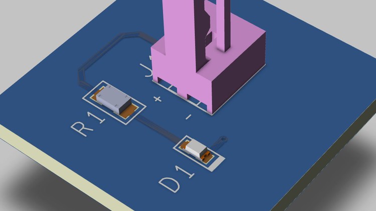
– Create a 3D model of your board
– Generate Bill of Material (BOM)
– Create assembly drawings showing position of components on the board
– Generate Gerber files, Pick and Place, Drill file and other files needed for manufacturing
Content